- 您现在的位置:买卖IC网 > Sheet目录3882 > PIC18F4539T-I/ML (Microchip Technology)IC MCU FLASH 12KX16 EE A/D 44QFN
2002 Microchip Technology Inc.
Preliminary
DS30485A-page 133
PIC18FXX39
16.3.8
SLEEP OPERATION
In Master mode, all module clocks are halted and the
transmission/reception will remain in that state until the
device wakes from SLEEP. After the device returns to
Normal mode, the module will continue to transmit/
receive data.
In Slave mode, the SPI transmit/receive shift register
operates asynchronously to the device. This allows the
device to be placed in SLEEP mode and data to be
shifted into the SPI transmit/receive shift register.
When all 8 bits have been received, the MSSP interrupt
flag bit will be set and if enabled, will wake the device
from SLEEP.
16.3.9
EFFECTS OF A RESET
A RESET disables the MSSP module and terminates
the current transfer.
16.3.10
BUS MODE COMPATIBILITY
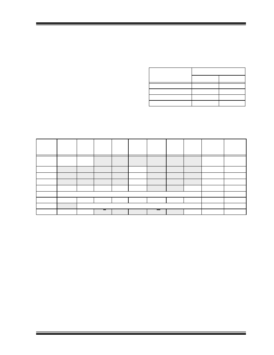
Table 16-1 shows the compatibility between the
standard SPI modes and the states the CKP and CKE
control bits.
TABLE 16-1:
SPI BUS MODES
There is also an SMP bit which controls when the data
is sampled.
TABLE 16-2:
REGISTERS ASSOCIATED WITH SPI OPERATION
Standard SPI Mode
Terminology
Control Bits State
CKP
CKE
0, 0
0
1
0, 1
0
1, 0
1
1, 1
1
0
Name
Bit 7
Bit 6
Bit 5
Bit 4
Bit 3
Bit 2
Bit 1
Bit 0
Value on
POR, BOR
Value on
All Other
RESETS
INTCON
GIE/GIEH
PEIE/
GIEL
TMR0IE
INT0IE
RBIE
TMR0IF
INT0IF
RBIF
0000 000x
0000 000u
PIR1
PSPIF(1)
ADIF
RCIF
TXIF
SSPIF
—
TMR2IF
TMR1IF
0000 0000
PIE1
PSPIE(1)
ADIE
RCIE
TXIE
SSPIE
—
TMR2IE
TMR1IE
0000 0000
IPR1
PSPIP(1)
ADIP
RCIP
TXIP
SSPIP
—
TMR2IP
TMR1IP
0000 0000
TRISC
TRISC7
TRISC6
TRISC5
TRISC4
TRISC3
*
TRISC0
1111 1111
SSPBUF
Synchronous Serial Port Receive Buffer/Transmit Register
xxxx xxxx
uuuu uuuu
SSPCON
WCOL
SSPOV
SSPEN
CKP
SSPM3
SSPM2
SSPM1
SSPM0
0000 0000
TRISA
—
PORTA Data Direction Register
-111 1111
SSPSTAT
SMP
CKE
D/A
P
S
R/W
UA
BF
0000 0000
Legend: x = unknown, u = unchanged, - = unimplemented, read as '0'. Shaded cells are not used by the MSSP in SPI mode.
* Reserved bits; do not modify.
Note 1: The PSPIF, PSPIE and PSPIP bits are reserved on the PIC18C2X2 devices; always maintain these bits clear.
发布紧急采购,3分钟左右您将得到回复。
相关PDF资料
PIC18LF2539T-I/SO
IC MCU FLASH 12KX16 EE AD 28SOIC
PIC18LF4539T-I/PT
IC MCU FLASH 12KX16 EE AD 44TQFP
PIC16LF874AT-I/ML
IC MCU FLASH 4KX14 A/D 44QFN
PIC16F77T-E/ML
IC MCU FLASH 8KX14 A/D 44QFN
PIC16F874A-E/ML
IC MCU FLASH 4KX14 A/D 44QFN
PIC16F74T-I/ML
IC MCU FLASH 4KX14 A/D 44QFN
PIC16F77T-I/ML
IC MCU FLASH 8KX14 A/D 44QFN
PIC18F24K20-I/SS
IC PIC MCU FLASH 8KX16 28SSOP
相关代理商/技术参数
PIC18F4539T-I/PT
功能描述:8位微控制器 -MCU 24KB 1408 RAM 32 I/O RoHS:否 制造商:Silicon Labs 核心:8051 处理器系列:C8051F39x 数据总线宽度:8 bit 最大时钟频率:50 MHz 程序存储器大小:16 KB 数据 RAM 大小:1 KB 片上 ADC:Yes 工作电源电压:1.8 V to 3.6 V 工作温度范围:- 40 C to + 105 C 封装 / 箱体:QFN-20 安装风格:SMD/SMT
PIC18F4550EPT
制造商:Microchip Technology Inc 功能描述:
PIC18F4550-I/ML
功能描述:8位微控制器 -MCU 32kBF 2048RM FSUSB2 RoHS:否 制造商:Silicon Labs 核心:8051 处理器系列:C8051F39x 数据总线宽度:8 bit 最大时钟频率:50 MHz 程序存储器大小:16 KB 数据 RAM 大小:1 KB 片上 ADC:Yes 工作电源电压:1.8 V to 3.6 V 工作温度范围:- 40 C to + 105 C 封装 / 箱体:QFN-20 安装风格:SMD/SMT
PIC18F4550-I/P
功能描述:8位微控制器 -MCU 32kBF 2048RM FSUSB2 RoHS:否 制造商:Silicon Labs 核心:8051 处理器系列:C8051F39x 数据总线宽度:8 bit 最大时钟频率:50 MHz 程序存储器大小:16 KB 数据 RAM 大小:1 KB 片上 ADC:Yes 工作电源电压:1.8 V to 3.6 V 工作温度范围:- 40 C to + 105 C 封装 / 箱体:QFN-20 安装风格:SMD/SMT
PIC18F4550-I/PT
功能描述:8位微控制器 -MCU 32kBF 2048RM FSUSB2 RoHS:否 制造商:Silicon Labs 核心:8051 处理器系列:C8051F39x 数据总线宽度:8 bit 最大时钟频率:50 MHz 程序存储器大小:16 KB 数据 RAM 大小:1 KB 片上 ADC:Yes 工作电源电压:1.8 V to 3.6 V 工作温度范围:- 40 C to + 105 C 封装 / 箱体:QFN-20 安装风格:SMD/SMT
PIC18F4550T-I/ML
功能描述:8位微控制器 -MCU 32kBF 2048RM FSUSB2 RoHS:否 制造商:Silicon Labs 核心:8051 处理器系列:C8051F39x 数据总线宽度:8 bit 最大时钟频率:50 MHz 程序存储器大小:16 KB 数据 RAM 大小:1 KB 片上 ADC:Yes 工作电源电压:1.8 V to 3.6 V 工作温度范围:- 40 C to + 105 C 封装 / 箱体:QFN-20 安装风格:SMD/SMT
PIC18F4550T-I/PT
功能描述:8位微控制器 -MCU 32kBF 2048RM FSUSB2 RoHS:否 制造商:Silicon Labs 核心:8051 处理器系列:C8051F39x 数据总线宽度:8 bit 最大时钟频率:50 MHz 程序存储器大小:16 KB 数据 RAM 大小:1 KB 片上 ADC:Yes 工作电源电压:1.8 V to 3.6 V 工作温度范围:- 40 C to + 105 C 封装 / 箱体:QFN-20 安装风格:SMD/SMT
PIC18F4553-I/ML
功能描述:8位微控制器 -MCU 32KB FLSH 2048 RAM FSUSB 2.0 12B ADC RoHS:否 制造商:Silicon Labs 核心:8051 处理器系列:C8051F39x 数据总线宽度:8 bit 最大时钟频率:50 MHz 程序存储器大小:16 KB 数据 RAM 大小:1 KB 片上 ADC:Yes 工作电源电压:1.8 V to 3.6 V 工作温度范围:- 40 C to + 105 C 封装 / 箱体:QFN-20 安装风格:SMD/SMT